


Wafer Surface Evaluation - Vision inspection
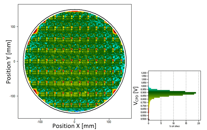
In semiconductor manufacturing, evaluating wafer cross-section roughness is challenging with traditional image processing. Our client needed an accurate, automated solution to detect surface defects. We built a deep learning system using PaDiM and ResNet-50, trained only on normal samples, to identify anomalies in wafer surfaces—enabling fast, precise, and scalable quality control in production.
Client Problem:
Detect defects on the cross-section of semiconductor wafers. These cross-sections may not be flat and may have rough spots. It is necessary to assess the overall roughness of the whole cutting plate.
Challenge:
Flat or rough or convex cross-section is a judgment based primarily on perception and are difficult to measure.
Using only traditional image processing methods such as measuring brightness, contrast and/or gradient are difficult to evaluate the roughness.
Tech Stack: PyTorch (framework); ResNet-50 (backbone); PaDim (anomaly detection)
Our Solution:
Using Anomaly Detection (Deep Learning) algorithms: Apply to surface images with uniform properties or mesh structure. Areas that are heterogeneous or structurally distinct are considered abnormal regions. The advantage of this approach is that it only needs to train the model with good samples.
Case studies

Intelligent Document Processing with AI Agent and OCR on Azure
Tinhvan Software built an Azure-based AI Agent and OCR tool to automate document search and image text extraction, enabling fast, secure, and structured data access. We developed an intelligent AI Agent and OCR pipeline to help enterprises query internal documents using natural language and extract structured data from image files. Built on Azure with infrastructure-as-code, the solution improves knowledge access, streamlines document processing, and enhances efficiency through secure, scalable cloud-native architecture.

Machine Learning System for Geophysical Reservoir Property Prediction (Phase 2)
Tinhvan Software built a machine learning platform to help geologists automate reservoir property analysis. The solution uses boosting models, domain-specific preprocessing, and interactive visualizations—empowering experts to interpret large-scale geophysical data faster and more accurately, with minimal technical overhead.

Petrology Prediction Model – AI for Geoscience (Phase 1)
Petrology Prediction Model, developed by Tinhvan Software for the Vietnam Petroleum Institute, applies machine learning to well log and core sample data, enabling accurate geological insights while reducing reliance on costly manual sampling and accelerating model testing in real-world exploration.